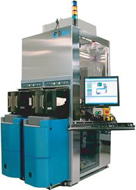
Debond and Cleave (DB&C) Tool
The DB&C tool is a small footprint tool designed for layer transfer applications in high-volume manufacturing.
Applications:
- SOI (silicon-on-insulator) is Used to reduce device voltage operation and power consumption and improve device speed.
- DSB (direct silicon bond) Improved device mobility in CMOS circuitry by providing separate crystal orientation layers for NMOS and PMOS.
- SOQ (silicon-on-quartz) Transferred single-crystal silicon onto a quartz substrate used for RF, display, and optical applications.
- SOG (silicon-on-glass) Transferred single-crystal silicon onto bulk glass, enabling low-cost, high-efficiency solar cells, displays, and optical applications.
- CSS (customer-specific substrate): A combination of donor-layer materials on unique handle substrates, including III-V and II-VI donor materials, sapphire ceramics, and flexible handle substrates.
The process is a dynamic, low-stress cleave action in which a donor layer transfers to a handle wafer at room temperature. SiGen's proprietary cleave technology combines a cleave initiation action followed by programmed propagation that optimizes cleave quality and uniformity.
Additional info
Debond & Cleave Tool (DB&C) (275KB PDF Format)