Solar Markets
With regards to the overall industry roadmap, there has been a general consensus that the wafer thickness will drop from the current levels of around 200um to levels around 150um in the next several years. Other major industry players are actively pursuing roadmaps, taking wafer thicknesses to 150um by 2010. The primary driver for this thickness reduction is the corresponding decrease in the amount of poly, with the resulting cost savings. SiGen provides thin wafers at a lower production cost, with enhanced wafer properties, benefiting the entire PV chain and driving to lower $/W.
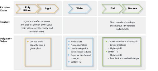
PolyMax Impact and Relevance
PolyMax Impact and Relevance There are multiple points of impact by the SiGen process which will lead to a $/W savings potential and which will impact a major segment of the PV market. The $/W savings are achieved by substantially lower wafering costs, by improving wafer attributes, and by both upstream and downstream cost savings potential.
It should be emphasized, however, that the wafers generated by the PolyMax™ approach show improved characteristics in terms of: reduced/eliminated micro-cracks, improved TTV, improved strength, and improved handling capability. These properties allow for better yield with downstream processing. With regards to upstream — since the PolyMax™ approach can produce the same number of wafers with roughly half the starting material — a correspondingly lower number of equipment is needed for poly production to achieve a given wafer output.
The innovation is the revolutionary application of an ion beam implantation and a cleave process to generate PV wafers repeatably, independent of diameter and with the ability to vary the thickness from 150um to sub-100um and down to 20um wafers. The innovation allows for the extension of wafering beyond any of the capabilities of the WireSaw with an elimination of consumables and waste materials.