Semiconductor Foundational Technology
Over the past 10 years, sigen has aggressively developed a rich set of technologies, which are reflected in almost 100 patents for layer transfer technology, equipment, and processes.

The basis for this development is the firm belief that next-generation devices will be built on engineered substrates to meet the ever-increasing demands of performance, power consumption, and heat dissipation.
EXAMPLES
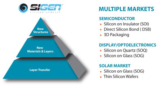
- SOI (silicon on insulator)
Used to reduce device voltage operation and power consumption to improve device speed. - DSB (direct silicon bond)
Improved device mobility in CMOS circuitry by providing separate crystal orientation layers for NMOS and PMOS. - SOQ (silicon on quartz)
Transferred single-crystal silicon onto a quartz substrate used for RF, display, and optical applications. - SOG (silicon on glass)
Transferred single-crystal silicon onto bulk glass, enabling low-cost, high-efficiency solar cells, displays, and optical applications. - CSS (customer specific substrate)
A combination of donor-layer materials on unique handle substrates, including III-V and II-VI donor materials and sapphire, ceramics, and flexible handle substrates.
Layer Transfer Technology Processes The company's proprietary NanoCleave® (Layer Transfer), NanoBond (Plasma-activated bonding), and NanoSmooth (EpiSmoothing/Epi Thickening) process steps have allowed SiGen to become a leading provider of innovative-engineered substrates through its process and technology: enabling its customers to develop new applications with greater functionality and higher speed, while improving cost, power efficiency, and heat dissipation.